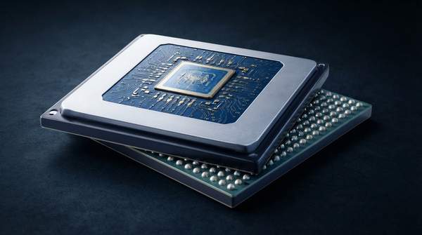
Advanced packaging technologies like 3D stacking and chiplets are critical for enhancing performance scaling and heterogeneous integration in modern high-performance computing (HPC) and artificial intelligence (AI) accelerators. These innovations address the limitations of traditional two-dimensional (2D) semiconductor scaling by enabling denser integration, higher bandwidth, and improved power efficiency, according to industry insights from Chiplet Marketplace and VIEW Micro Metrology.
The shift to advanced packaging is driven by the increasing demands of AI and HPC workloads, which require unprecedented levels of die-to-die bandwidth, often reaching multi-terabyte-per-second territory, as noted by Cadence Design Systems in a Chiplet Marketplace article. Understanding the architectural benefits and trade-offs of these technologies is essential for informed hardware design and evaluation.
Technical Principles of 3D Stacking and High-Bandwidth Memory (HBM)
3D Integrated Circuits (3D ICs) represent a fundamental shift from traditional planar chip designs by stacking multiple layers of silicon dies vertically. This vertical integration allows for the dense combination of different functionalities, such as logic, memory, and input/output (I/O) components, within a compact footprint, explains Tessolve in a Chiplet Marketplace article. The core of 3D IC integration relies on advanced interconnect strategies that ensure seamless interaction between these stacked dies.
Key to this vertical interconnection are Through-Silicon Vias (TSVs), micro-bumps, and hybrid bonding. TSVs are vertical electrical connections that pass directly through a silicon die, enabling short-distance communication between stacked layers. Micro-bumps are tiny metallic connections that link the pads of one die to another, while hybrid bonding offers direct copper-to-copper connections, further enhancing signal integrity and power efficiency, according to Cadence Design Systems. This architecture significantly reduces the physical distance signals must travel, leading to substantial improvements in performance and power consumption.
High-Bandwidth Memory (HBM) is a prominent example of 3D stacking in action. HBM stacks multiple DRAM dies vertically, connecting them to a base logic die using TSVs. This configuration creates an ultra-high-bandwidth memory solution that is crucial for data-intensive applications in HPC and AI accelerators, where feeding data-hungry compute engines efficiently is paramount, as highlighted by Tessolve.