As the quest to build large-scale, fault-tolerant quantum computers accelerates, researchers face a fundamental scaling challenge: controlling millions of quantum bits, or qubits, which must operate at temperatures colder than deep space. The solution emerging as a critical enabling technology is the development of cryogenic complementary metal-oxide-semiconductor (cryo-CMOS) circuits. By allowing control electronics to move from room-temperature racks into the cryogenic environment alongside the qubits, cryo-CMOS integrated circuits directly address the wiring, power, and complexity bottlenecks that have constrained the growth of quantum processors, particularly for systems based on superconducting and semiconductor qubits.
The Imperative for Cryo-CMOS in Quantum Computing
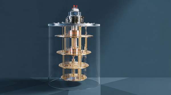
The development of practical, large-scale quantum computers is fundamentally an integration problem. According to the IEEE Solid-State Circuits Society, scaling a fault-tolerant machine to the millions of qubits needed for useful algorithms presents a "daunting challenge." A primary obstacle, identified in multiple technical analyses, is the "wiring bottleneck." Conventional systems rely on a vast number of coaxial cables running from room-temperature control hardware down through the stages of a dilution refrigerator to the quantum processor. This approach is not scalable; for every qubit, multiple control and readout lines are needed, and the sheer volume of wires introduces a significant heat load into the cryogenic system, limiting the number of qubits that can be effectively managed and threatening their delicate quantum states.
Cryo-CMOS technology offers a path to circumvent this critical bottleneck. By designing CMOS chips—the same technology found in modern classical computers—to function reliably at cryogenic temperatures around 4 Kelvin, engineers can place the control and readout electronics in close proximity to the qubits. This co-location dramatically reduces the complexity and heat load of the interconnects between temperature stages. Instead of thousands of individual wires penetrating the cryostat, a few digital lines can communicate with a complex cryo-CMOS System-on-Chip (SoC) that manages a large array of qubits, paving the way for the dense, integrated control systems required for future quantum computing architectures.
Primary Technical Challenges of Cryogenic CMOS Operation
Transitioning sophisticated electronics from room temperature to the extreme cold of a quantum computer's core introduces a unique set of engineering hurdles. The first is managing power dissipation. All electronics generate heat, but inside a cryostat, this thermal load is a critical constraint. The limited cooling power of dilution refrigerators means that the total power consumption of any electronics operating inside must be minimized. According to an IEEE presentation, the power budget is often just a few milliwatts per control channel to support a growing number of qubits at the 4 Kelvin stage. Exceeding this budget would overwhelm the cooling system and destroy the fragile quantum states of the qubits.
A second major challenge is ensuring signal fidelity. Qubit operations are extremely sensitive to electrical noise. To achieve the high fidelity required for fault-tolerant computation—often cited as greater than 99.99%—control signals must be exceptionally clean. This translates to stringent requirements for the cryo-CMOS electronics, including a high Spur-Free Dynamic Range (SFDR) of more than 45 dB to prevent spurious signals from corrupting qubit operations. Finally, the fundamental behavior of CMOS devices and materials changes at cryogenic temperatures. Addressing these "material challenges," as one analysis notes, is essential for designing reliable and high-performance circuits, requiring innovative approaches to analog, digital, and RF circuit design.
Cryo-CMOS Challenges and Solutions for Qubit Control
Successfully operating complex electronics in a cryogenic environment requires targeted solutions to the unique hurdles posed by wiring, power, and signal fidelity. Overcoming these challenges is essential for integrating control systems that can manage thousands or millions of qubits without compromising their performance.
| Technical Challenge | Description of Problem | Architectural/Circuit Solution |
|---|---|---|
| Wiring Bottleneck | Connecting room-temperature electronics to a growing number of cryogenic qubits requires an unsustainable number of individual wires, which introduces excessive heat and limits system size. This is a key bottleneck for large-scale quantum computers. | Cryo-CMOS integrated circuits (ICs) are designed to operate at cryogenic temperatures, allowing control electronics to be placed near the qubits and drastically reducing the number of wires needed between temperature stages. |
| Power Dissipation | All electronics generate heat, but within a cryostat, this thermal load is a critical constraint. The limited cooling power of dilution refrigerators restricts the total power consumption of any electronics operating inside, which in turn limits the number of control channels. | Engineers are developing low-power cryo-CMOS designs and integrating them into System-on-Chip (SoC) architectures. This approach minimizes power consumption per channel, allowing more controllers to operate within the cryostat's strict thermal budget. |
| Noise and Fidelity | Qubit operations are extremely sensitive to electrical noise. To achieve the high fidelity required for fault-tolerant computation—often cited as greater than 99.99%—control signals must be exceptionally clean, with a high Spur-Free Dynamic Range (SFDR). | Cryo-CMOS control systems incorporate high-precision digital-to-analog converters (DACs) and dedicated microcontrollers. These components enable low-noise, low-power flux biasing, a technique optimized for executing high-fidelity two-qubit gates. |
Architectural Solutions: From Integrated Circuits to Hybrid Systems
A leading architectural solution for the challenges of cryogenic control is the System-on-Chip (SoC). According to a presentation for the IEEE Solid-State Circuits Society, complex SoCs with digital, analog, and RF capabilities can be integrated with sufficiently low power consumption to be compatible with the cooling capacity of dilution refrigerators. By combining multiple functions onto a single chip, SoCs reduce the system's physical footprint and power draw, both of which are critical for scalability. This integration is a long-term goal for researchers, as it directly addresses the need to increase the number of control channels while staying within the power limits of the cryogenic platform.
While a fully integrated SoC represents a future goal, a more practical near-term approach is a hybrid architecture. This strategy combines specialized cryo-CMOS components close to the qubits with more complex electronics at a warmer stage or at room temperature. IBM Research, for instance, has developed a hybrid control solution for its superconducting qubit processors. This system uses cryo-CMOS application-specific integrated circuits (ASICs) for precise, low-noise qubit control, which are thermally anchored inside the cryostat. These cryogenic components handle sensitive, high-fidelity operations while interfacing with other electronics outside the coldest environment. IBM reports that this hybrid architecture is a viable path toward reducing the size, power, and cost of control systems, which is central to delivering fault-tolerant quantum computers.
Tailoring Control for Leading Qubit Platforms
The design of cryo-CMOS controllers must be tailored to the specific needs of different qubit technologies. For superconducting qubits, a leading platform, control systems must provide what IBM Research describes as "low-noise, low-power flux biasing" to manipulate qubit states and perform high-fidelity two-qubit gates. IBM's system, for example, integrates a microcontroller and high-precision digital-to-analog converters (DACs) into its cryo-CMOS ASICs to meet these precise demands, with each ASIC supporting 16 independently programmable channels.
Similarly, silicon spin qubits are another promising technology, valued for their "transistor-like footprint and compatibility with industrial silicon manufacturing," as noted by the IEEE Solid-State Circuits Society. This compatibility suggests a more direct path to leveraging mature semiconductor fabrication techniques for building large-scale quantum processors. For both platforms, the fundamental requirements for the control electronics are similar: achieving high operational fidelity of over 99.99% requires the controller chip to exhibit low noise and a Spur-Free Dynamic Range (SFDR) greater than 45 dB, all while keeping power consumption to a few milliwatts per channel to manage the thermal load at the 4 Kelvin stage.
Enabling Scalable Quantum Computing with Cryo-CMOS
Cryo-CMOS integrated circuits are essential for overcoming the scaling challenges of quantum processors by enabling control electronics to operate directly at cryogenic temperatures. This technological shift directly confronts the wiring and power consumption bottlenecks that have historically limited the size and complexity of quantum systems. As research progresses, the viability of this approach will be demonstrated by key advancements. The key metric to watch will be the increased integration density of cryo-CMOS control channels per qubit and demonstrated fault-tolerant operation of larger qubit arrays.
Sources
- Ieeexplore
- Quantum Computing: Challenges of Cryogenic CMOS Controller for Qubits — IEEETV
- Semanticscholar
- Cryo-CMOS Integrated Circuits for Silicon Qubits in the Quantum Computing Stack — IEEE Solid-State Circuits Society
- A Cryo-CMOS Control System for Large-Scale Superconducting Qubit Quantum Computing — IBM Research